Via Tenting: A Comprehensive Guide to PCB Design and Manufacturing Techniques
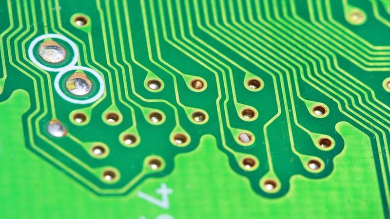
Vias are small holes in a PCB that enable electrical connections between different layers of the board. In the context of PCB design, via tenting refers to the process of covering the vias with a protective layer, typically a solder mask or dry film. This protective layer shields the vias from environmental factors, such as […]