Metal Core PCB (MCPCB): Revolutionizing Thermal Management in Electronics
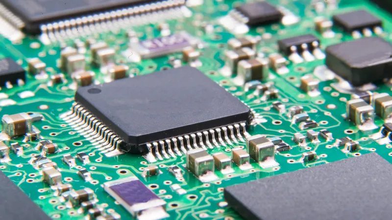
This article delves into the technology behind Metal core PCBs (MCPCBs), recent advancements, practical engineering applications, and the challenges faced in their implementation. Introduction The miniaturization and ever-increasing power demands of modern electronics create a significant challenge: thermal management. Traditional printed circuit boards (PCBs) often struggle to dissipate heat effectively, leading to component overheating and potential system failure. […]
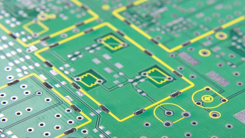
Trace Width vs Current in PCB Design
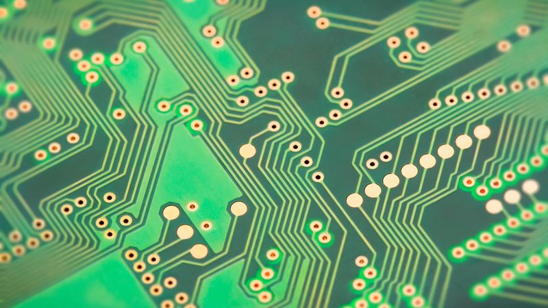
This article explores the key factors influencing trace width, provides practical guidelines, and highlights best practices for selecting the correct dimensions based on current-carrying demands in modern PCB design. Traces on a Printed Circuit Board (PCB) Introduction PCB trace width refers to the physical width of the copper pathways on a printed circuit board that carries electrical current. It […]
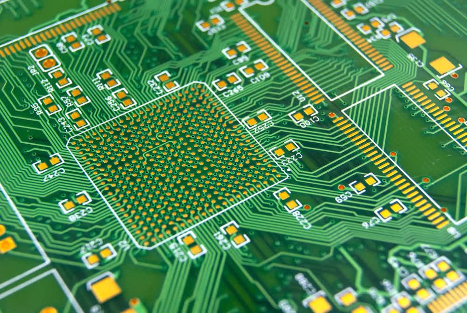
PCB Material: A Comprehensive Guide to Understanding and Choosing the Right Materials
This comprehensive guide will cover the basics of PCB materials, the different types of materials available, their properties, and choosing the right material for your application. Batch of green printed circuit boards with components etched on it Introduction Printed Circuit Board (PCB) materials form the foundation of electronic circuits, serving as the mechanical backbone and the electrical […]
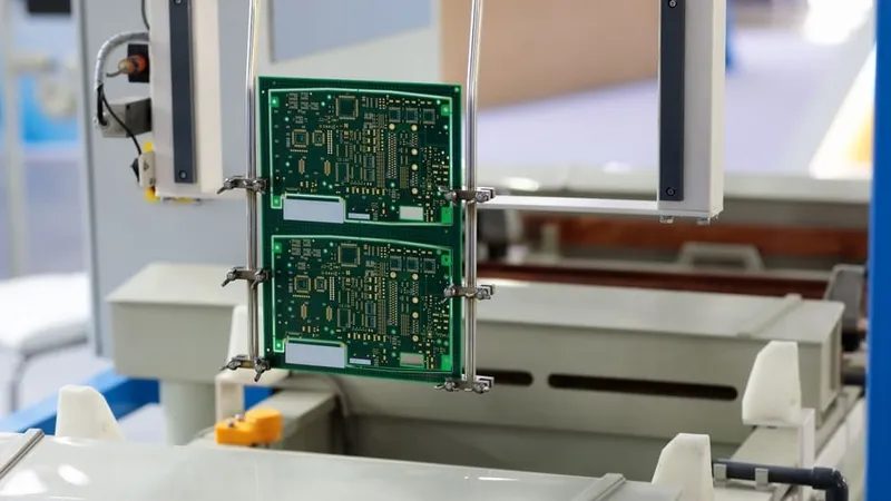
Solder Reflow: An In-Depth Guide to the Process and Techniques
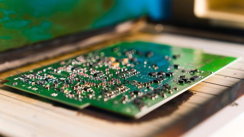
This article provides a detailed overview of the solder reflow process, types of reflow ovens, temperature profiles, solder paste composition and selection, reflow process potential challenges, solutions, inspection, and quality control techniques. Reflow soldering furnace used on mounted PCB Introduction Solder reflow is a critical process in the electronics industry, primarily used to attach surface-mount […]
PCB Surface Finish: The Ultimate Guide to Understanding and Choosing the Right Option
This guide dives deep into the world of PCB surface finishes: In this article, you will experience a comprehensive analysis of various types, factors for optimal performance, and comparing different PCB finishes to choose right one for your specific application Introduction In the intricate world of Printed Circuit Board (PCB) production, surface finish stands […]
PCB Solder Mask: Everything You Need to Know
The purpose of this article is to provide a comprehensive, in-depth guide to PCB soldermask, exploring the key concepts, principles, and practical applications that will help you excel in PCB design and manufacturing. Introduction Solder mask, the thin polymer layer applied to printed circuit boards (PCBs), plays a crucial role in modern electronics manufacturing. This […]
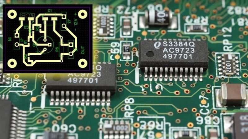
PCB Silkscreen: What is it?
The silkscreen is a layer on the surface of a PCB that is used to identify a lot of information about the electronic printed circuit board. Silkscreen layer of a PCB in the view (green color) Introduction PCB silkscreen is an integral part of circuit board design. It serves as a communicative layer in PCB […]
What are Gerber Files? Understanding the Blueprint of Electronics Manufacturing
This article provides an in-depth view of Gerber files, including their origin, structure, and role in PCB design and manufacturing processes. Gerber File Schematic in PCB Manufacturing What are Gerber Files? Gerber files are essential in the electronics manufacturing industry. These files are essentially the blueprint that guides the production of printed circuit boards (PCBs), found […]