PCB X ray inspection means using an x ray machine to examine printed circuit boards. X rays are extremely high-frequency and high-energy electromagnetic waves of very short lengths, shorter than those of visible light. These waves can penetrate solid objects.
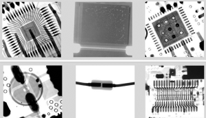
In the world of electronics, manufacturers use the penetrability of x rays to view hidden features of printed circuit boards. For example, with X ray inspection, PCB components such as BGA and high-density IC connections can be checked for misalignment and other problems.
More importantly, x ray inspection allows quality control technicians to view solder joints and inspect them for flaws. This helps catch defects that would otherwise go unnoticed due to their hidden nature. Here is how PCB X ray inspection works:
- Heavy or high-density materials absorb x-rays more than lighter materials.
- On a PCB, the solder alloy carries heavier materials. These absorb more x-rays than components and other parts of the board.
- When X rays are shone on a sample PCB, therefore, only a few will go through the soldered parts
- A detector, with the help of special software, utilizes the varied absorption of the x rays to create a picture of the PCB; much like it does when scanning bones.
- The soldered areas appear dark, while other parts appear bright. This image is cast on a computer screen.
- When a defect is present, a discrepancy in the light and dark areas will appear, such as shadows in the pins and pads.
- The inspecting technician views this image to find defective soldered areas or components, thereby ensuring high-quality production.
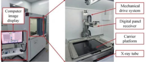
X ray PCB machine and its constituent components
PCB X Ray Advantages
In the electronic industry, its standard practice to use an x ray machine for PCB inspection. This is useful when it comes to critical circuits boards, such as those used in medical, military and aerospace applications. PCB x ray inspection, when compared to visual inspection and other examination methods, offers several unique benefits.
- No Damage: X ray inspection is non-invasive and non-destruction. No parts of the board or its assembled components are damaged or destroyed during the process.
- Hidden Flaws: unlike the visual method, x ray PCB inspection can help view parts of the board that are hidden from view, such as inner layers or BGA and IC connections.
- Flexible Examination: with ability to create either 2D or 3D view of the PCB structure, x ray inspection provides the flexibility needed to analyze different type of circuit boards as per the required levels of visualization.
- Higher Accuracy: X ray PCB inspection offers greater accuracy when compared to other techniques such as the use of magnifying pieces or microscopes and AOI. It gives a clear analysis of the solder joints, component connections, and other important information needed to ensure a thorough inspection.
- Failure Analysis: using the information of x ray inspection, engineers can analyze defects and effectively find their root causes. That means better quality PCBs based on practical improvements.