Quick turn PCBs are designed, fabricated, and assembled swiftly, ensuring tight schedules and deadlines are met, even for high-volume orders. This article investigates the quick turn PCB process, highlighting its benefits, stages, and how it guarantees quality within a short turnaround time.
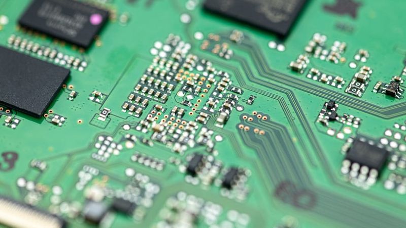
High-tech electronic PCB with processor and microchips
Introduction
In the fast-paced world of electronics development, where time-to-market is a crucial determinant of a product’s success, quick turn PCB assembly has emerged as a pivotal innovation. These rapidly produced printed circuit boards (PCBs) are transforming the prototyping process, enabling engineers to create and refine PCB prototypes with unmatched speed and efficiency. By leveraging advanced manufacturing techniques, quick turn PCBs significantly reduce production time—from several weeks to just a few days, or even hours in certain scenarios—addressing the critical need for rapid prototyping in the industry.
This swift turnaround is not just about speed; it’s about enabling companies to stay ahead of the competition and quickly adapt to shifting market demands. The ability to iterate and test designs rapidly means that engineers can identify and rectify potential issues early in the development process, ensuring higher quality and reliability in the final product. Adhering to IPC standards throughout the PCB assembly process also guarantees that these quick turn boards meet stringent quality and performance benchmarks, despite the accelerated timeline.
By incorporating quick turn PCBs into their development cycles, companies can optimize their product designs more efficiently, reduce time-to-market, and ultimately achieve greater success in the competitive electronics marketplace.
The Essence of Quick Turn PCBs: Speed Meets Precision
Quick turn PCBs’ significance in the electronics industry lies in the ability to accelerate PCB prototypes and allow for faster design iterations, which is crucial in an ever-evolving field where speed to market can determine a product’s success.
The key differences between quick turn PCBs and traditional PCB manufacturing revolve around speed, flexibility, and production volume. Quick turn PCB services prioritize rapid prototyping and short lead times.. In contrast, traditional methods focus on larger production runs and may take substantially longer to produce boards, often resulting in longer time-to-market schedules. Quick turn services usually accommodate smaller batch sizes, which benefit design modifications that come from testing and feedback cycles.
Due to quick turn, the entire PCB assembly and fabrication process can be done in a short time. The turnaround time for a quick turn rigid PCB is as low as 24 hours, while flex and rigid-flex PCBs may require about 7 days turnaround time. This is due to board and design complexities in terms of design specifications, surface finish, number of layers or board stack up, mounting techniques (SMT or Through hole), and lamination. This expedited timeline is significantly shorter compared to traditional PCB manufacturing, where lead times can extend from one to several weeks. Quick turn services can often meet stringent deadlines required by industries that demand rapid responses to design changes.
Projects that benefit the most from quick turn PCB services often include PCB prototypes, custom designs, and limited production runs where rapid testing and iteration are critical. Fields such as consumer electronics, medical devices, and telecommunications frequently utilize quick turn services to accommodate fast-moving project timelines and last-minute design changes. Engineers require quick feedback on performance and designs to stay competitive, making these quick turn services essential.
Limitations and Constraints of Quick Turn PCB Manufacturing
While quick turn PCB manufacturing delivers substantial benefits in terms of speed, it is not without its limitations and constraints:
-
Cost: The accelerated production process often incurs a higher per-unit cost compared to traditional manufacturing methods.
-
Volume Limitations: Quick turn services are generally optimized for smaller production runs and may not be economically viable for large-scale manufacturing.
-
Design Complexity: Complex designs involving multiple layers or exotic materials may not be suited for the fastest turnaround options.
-
Material Availability: To meet rapid turnaround times, material choices may be restricted to those readily available in stock.
-
Quality Trade-offs: Despite stringent quality control measures, the expedited process might occasionally result in minor imperfections that would be identified in longer production cycles.
This table simplifies the difference between quick turn PCBs and traditional PCB manufacturing in terms of time, cost, and complexity:
|
Aspect |
Quick Turn PCBs |
Traditional PCB Manufacturing |
|
Lead Time |
24 hours to a few days |
1 to 8 weeks |
|
Cost |
Higher per unit, low setup cost |
Lower per unit, high setup cost |
|
Fleksibilitet |
High (small batches) |
Low (large batches required) |
|
Design Iteration |
Fast due to quick turns |
Slower, more rigid process |
|
Typical Use Cases |
Prototyping, limited runs |
Mass production |
The Quick Turn PCB Manufacturing Process
The quick turn PCB manufacturing process is a highly efficient and streamlined approach as it involves several key steps, each optimized for speed and precision:
1. Design Creation
The process begins with creating a PCB design using specialized Computer-Aided Design (CAD) software. This software allows engineers to define the PCB layout, including component placement, trace routing, and layer stack-up. Advanced CAD tools often include design rule-checking (DRC) features that help catch potential issues early in the process.
2. Design Verification
Once the design is complete, it undergoes rigorous verification. This step involves checking for errors or issues that could affect manufacturability or functionality. Automated verification tools scan the design for violations of design rules, ensuring that the PCB meets manufacturing specifications and electrical requirements.
3. Fabrication Preparation
After verification, the design is converted into a set of Gerber files. These files contain all the necessary information for PCB fabrication, including copper layer data, solder mask, silkscreen, and drill information. Advanced software streamlines this conversion process, reducing the chance of errors and speeding up the transition from design to fabrication.
4. Production Setup
With the Gerber files in hand, the production equipment is configured according to the specifications. This step involves programming CNC machines, setting up etching equipment, and preparing drilling and plating systems. Automated setup processes significantly reduce the time required for this stage.
5. PCB Fabrication
The actual fabrication of the PCB involves several sub-processes:
-
Etching: Precise chemical or laser etching removes unwanted copper from the board.
-
Drilling: High-speed CNC machines drill holes for vias and component mounting.
-
Plating: Copper plating is applied to create conductive paths between layers.
-
Surface treatment: The board surface is prepared for component assembly.
Specialized equipment such as laser direct imaging (LDI) systems and advanced etching machines contribute to the speed and precision of this step.
6. Assembly
Components are soldered onto the fabricated PCBs. This can be done manually for prototypes or small runs, or via automated pick-and-place machines for larger quantities. Advanced assembly equipment can place thousands of components per hour, significantly reducing production time.
7. Testing
The final step involves thorough testing to ensure the PCB meets quality standards and functions correctly. Automated optical inspection (AOI) systems and flying probe testers quickly identify any defects or electrical issues.
Throughout this process, automation and advanced software play crucial roles in achieving faster quick turnaround times. Computer-controlled equipment, real-time monitoring systems, and integrated manufacturing execution systems (MES) optimize each step of the process, reducing human error and increasing efficiency.
Cutting-Edge Technologies Driving Quick Turn PCB Production
The field of quick turn PCB (Printed Circuit Board) production is experiencing a transformative shift driven by cutting-edge technologies that are reshaping the manufacturing process. These advancements are significantly enhancing speed, precision, and efficiency, setting new industry benchmarks.
Artificial Intelligence and Machine Learning
Artificial Intelligence (AI) and Machine Learning (ML) are at the forefront of this transformation. AI-powered Design Rule Checking (DRC) systems are revolutionizing PCB design by detecting potential flaws with exceptional accuracy and speed. Leveraging extensive databases of successful designs and manufacturing data, these systems continuously refine their detection capabilities, ensuring adherence to rigorous design rules and reducing errors. During production, ML algorithms optimize manufacturing parameters in real-time, adjusting for material variations and environmental conditions to maintain consistent quality.
Advanced Computer-Aided Design (CAD) and Computer-Aided Manufacturing (CAM) Software
The evolution of Computer-Aided Design (CAD) and Computer-Aided Manufacturing (CAM) software has streamlined both design and production processes. Modern CAD tools feature advanced auto-routing algorithms that expedite the creation of optimal trace layouts. Real-time collaboration features allow multiple engineers to work on the same design simultaneously, enhancing efficiency and fostering innovation. On the manufacturing side, advanced CAM software translates design files into machine instructions with minimal setup time and reduced human error, ensuring a smooth transition from design to production.
Innovative Materials and Components
Recent advancements in materials and components are further driving progress in PCB manufacturing. High-speed laminates now offer improved signal integrity, supporting higher clock speeds and denser layouts without sacrificing performance. Turnkey solutions incorporating embedded components, such as resistors and capacitors within the PCB layers, reduce assembly time and enhance reliability. Novel solder materials with faster cooling times and lower melting points are accelerating the reflow process in surface mount technology (SMT) assembly. Additionally, the use of multi-layer PCBs allows for more complex and compact designs, meeting the increasing demands of modern electronics. Standard PCB processes are also benefiting from these innovations, which contribute to more efficient and reliable production runs.
Key technologies driving quick turn PCB production include:
-
Laser Direct Imaging (LDI): Enables ultra-precise patterning of PCB layers without the need for photomasks, reducing production time and improving accuracy.
-
3D Printed Electronics: Allows for rapid prototyping of complex 3D-shaped PCBs and the integration of electronic circuits into 3D-printed objects.
-
Digital Twin Technology: Creates virtual replicas of production lines, enabling real-time monitoring, predictive maintenance, and process optimization.
-
Augmented Reality (AR) in Assembly: Guides technicians through complex assembly processes, reducing errors and training time.
-
Automated Optical Inspection (AOI) with AI: Enhances defect detection capabilities, reducing false positives and increasing inspection speed.
-
Additive Manufacturing for PCB Production: Enables the creation of complex PCB structures with fewer process steps, potentially reducing production time for certain designs.
-
Smart Factory Integration: Connects all aspects of the production process, from design to shipping, optimizing workflow and reducing lead times.
Automated Optical Inspection (AOI) in Quick Turn PCBs
Automated Optical Inspection (AOI) is essential for maintaining high-quality standards in the fast-paced environment of quick turn PCB assembly. As production speeds increase, the risk of defects and errors rises, making AOI a critical tool for ensuring circuit board assembly reliability and customer satisfaction.
Recent advancements in AOI technology have significantly boosted its effectiveness in high-quality PCB production. High-resolution cameras with multi-angle imaging capabilities can now detect defects as small as 10 micrometers. Machine learning algorithms have enhanced defect classification accuracy, minimizing false positives and reducing the need for manual inspections. Additionally, real-time data analytics integrated with AOI systems provide immediate feedback to the production line, facilitating rapid adjustments and continuous improvement.
These innovations in AOI technology are integral to sourcing high-quality PCBs that meet precise specs, supporting efficient and reliable quick turn PCB assembly processes.
AOI systems detect and classify defects through a sophisticated process:
-
Image Acquisition: High-resolution cameras capture detailed images of the PCB surface under controlled lighting conditions.
-
Image Processing: Advanced algorithms enhance image quality and isolate features of interest.
-
Feature Extraction: The system identifies key characteristics such as component placement, solder joint quality, and trace integrity.
-
Defect Detection: AI-powered algorithms compare the extracted features against a “golden sample” or predefined parameters to identify anomalies.
-
Defect Classification: Machine learning models categorize detected defects based on type, severity, and potential impact on functionality.
Statistics demonstrate the significant impact of AOI on quick turn PCB production:
-
Defect detection rates have improved by up to 99.5%, compared to 85-90% for manual inspection.
-
False positive rates have been reduced to less than 1%, down from 5-10% in earlier AOI systems.
-
Inspection time has decreased by 80% compared to manual methods, allowing for faster production cycles.
-
Overall production yield has increased by 15-20% in facilities implementing advanced AOI systems.
The table below compares traditional inspection methods with AOI:
|
Aspect |
Traditional Inspection |
Automated Optical Inspection |
|
Speed |
50-100 components/minute |
500-1000 components/minute |
|
Accuracy |
85-90% defect detection |
99-99.5% defect detection |
|
Consistency |
Varies with operator fatigue |
Consistent performance |
|
Cost |
High labor costs |
Higher initial investment, lower long-term costs |
|
Data Collection |
Limited, manual recording |
Comprehensive, automatic data logging |
|
Process Feedback |
Delayed, based on batch results |
Real-time, allowing immediate adjustments |
Optimizing Design for Quick Turn PCB Production
Optimizing PCB designs for quick turn PCB fabrication involves a strategic approach that balances speed, manufacturability, and performance. Engineers must carefully consider several factors to ensure that their designs are ideal for quick turn PCB assembly and production. Key considerations include controlled impedance for signal integrity, manufacturability for efficient quick turn PCB prototypes, and design adjustments to align with rapid production capabilities. Leveraging PCB assembly services and obtaining an instant quote can further streamline the process, ensuring that the final product meets both performance requirements and rapid turnaround expectations.
When designing for quick turn PCB production, consider the following:
-
Layer Count: Minimize the number of layers whenever possible. Two to four-layer boards are typically faster and more cost-effective to produce than multilayer boards.
-
Board Size: Opt for standard board sizes when feasible. Non-standard sizes may require additional setup time and costs.
-
Component Selection: Choose readily available components with standard footprints. Avoid parts with long lead times or custom requirements.
-
Trace Width and Spacing: Use wider traces and larger spacing where possible to improve manufacturability and yield.
-
Via Types: Stick to through-hole vias when possible. Blind and buried vias can significantly increase production time and cost.
-
Copper Weight: Standard 1 oz copper is typically the fastest option. Heavier copper weights may extend production time.
-
Surface Finish: Choose common finishes like HASL or ENIG for faster turnaround times.
Balancing complexity and manufacturability is crucial in quick turn designs. While it’s tempting to push the limits of technology, simpler designs often result in faster production and higher yields. Consider these strategies:
-
Modularize complex circuits: Break down complex designs into simpler sub-circuits that can be manufactured more easily.
-
Use standard design rules: Adhere to your manufacturer’s standard design rules rather than pushing for tighter tolerances.
-
Optimize component placement: Arrange components to minimize the need for complex routing and reduce the number of required layers.
-
Leverage Design for Manufacturing (DFM) tools: Utilize DFM software to identify and resolve potential manufacturing issues early in the design process.
Checklist of Best Practices for Quick Turn PCB Design:
-
Verify component availability and lead times
-
Use standard board sizes and thicknesses
-
Minimize layer count
-
Adhere to manufacturer’s standard design rules
-
Optimize component placement for efficient routing
-
Use readily available surface finishes
-
Include clear and complete silkscreen markings
-
Provide comprehensive design documentation
-
Perform thorough DRC and ERC checks
-
Validate design with DFM analysis tools
Common design pitfalls to avoid in quick turn PCB projects:
-
Overcomplicating the design with unnecessary features
-
Specifying non-standard materials or processes
-
Pushing the limits of manufacturing capabilities (e.g., extremely fine pitch components)
-
Neglecting to consider thermal management in high-power designs
-
Failing to account for signal integrity in high-speed designs
-
Overlooking regulatory compliance requirements
-
Inadequate clearance around mounting holes or board edges
-
Inconsistent or incomplete design documentation
-
Last-minute design changes without considering their impact on manufacturability
DFM Considerations for Quick Turn PCBs
Design for Manufacturability (DFM) is essential in quick turnaround PCB production, as it significantly influences the speed, cost, and quality of the manufacturing process. Applying DFM principles ensures that designs are optimized for rapid production, particularly when using PCB assembly services, while maintaining high yield rates and reducing potential manufacturing issues. This approach is critical for both standard PCBs and RoHS-compliant boards, ensuring that the quick turnaround process is efficient and produces high-quality results.
Specific DFM guidelines for quick turn PCBs include:
-
Standardization: Use standard board sizes, thicknesses, and materials to reduce setup time and costs.
-
Component Selection: Choose readily available components with standard footprints to avoid delays.
-
Trace and Space Requirements: Adhere to manufacturer-recommended minimum trace widths and spacings to ensure reliable production.
-
Via Design: Minimize the use of blind and buried vias, opting for through-hole vias when possible.
-
Copper Balance: Maintain even copper distribution across layers to prevent warping during manufacturing.
-
Silkscreen Design: Ensure clear, legible silkscreen markings that don’t overlap with solder pads.
-
Solder Mask Considerations: Use standard solder mask colors and avoid solder mask defined (SMD) pads for quick turn production.
DFM can significantly reduce production time and improve yield in several ways:
-
Simplified Tooling: Standardized designs require less custom tooling, reducing setup time.
-
Improved First-Pass Yield: DFM-optimized designs are less likely to have manufacturing defects, minimizing rework and scrap.
-
Faster Assembly: Properly spaced components and clear markings speed up the assembly process.
-
Reduced Testing Time: DFM principles often result in more testable designs, streamlining the quality control process.
The table below shows DFM considerations for Quick Turn vs. Traditional PCB Manufacturing
|
Aspect |
Quick Turn PCBs |
Traditional PCBs |
|
Board Size |
Standard sizes preferred |
More flexibility for custom sizes |
|
Layer Count |
2-6 layers typical |
Up to 30+ layers possible |
|
Via Types |
Through-hole preferred |
Greater use of blind/buried vias |
|
Trace/Space |
Wider traces and spaces |
Can accommodate finer geometries |
|
Component Density |
Moderate |
Can be very high |
|
Silkscreen |
Essential, must be clear |
Can be more detailed |
|
Material Selection |
Limited to common materials |
Wide range of specialty materials |
|
Copper Weight |
1 oz standard |
Multiple weights common |
|
Edge Plating |
Typically avoided |
More commonly used |
Several software tools can assist with DFM analysis for quick turn PCBs:
-
Mentor Graphics’ DFM Analysis: Offers comprehensive DFM checks and optimization suggestions.
-
Cadence Allegro DFM Checker: Provides real-time DFM feedback during the design process.
-
Altium Designer with DFM Rules: Incorporates DFM checks into the standard design workflow.
-
Solo PCB Design: Offers a dedicated DFM analysis module for quick turn PCB designs.
-
Easy Logix DFM Stream: Specializes in DFM analysis for high-speed and complex PCB designs.
Quality Control in Rapid Production: Ensuring Reliability
Quick turn PCB production poses distinct challenges in maintaining high-quality standards while adhering to tight deadlines. The accelerated timeline can increase the risk of errors, reduce inspection time, and create pressure to bypass critical quality checks. However, to ensure the reliability of the final product, it is essential to implement robust quality control measures. This includes adhering to ISO and IPC standards, ensuring RoHS compliance, and utilizing advanced circuit board assembly techniques. By doing so, manufacturers can deliver high-quality PCBs in the USA, Europe and globally, even within the constraints of quick turn PCB fabrication and assembly. Offering instant quotes further streamlines the process, enabling efficient project management from start to finish.
Key challenges in quick turn PCB quality control include:
-
Balancing speed with thorough inspection
-
Adapting to frequent design changes
-
Maintaining consistency across small batch sizes
-
Detecting defects in complex, high-density boards
-
Ensuring component quality in a fast-paced environment
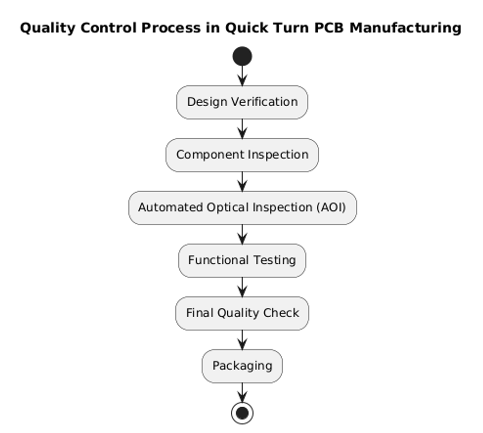
To address these challenges, quick turn PCB manufacturers employ several quality control measures:
-
Design Verification: Automated design rule checks (DRC) and design for manufacturability (DFM) analysis are performed to catch potential issues before production begins.
-
Component Inspection: Incoming components are verified for authenticity, specifications, and quality to prevent issues downstream.
-
Automated Optical Inspection (AOI): High-speed cameras and advanced image processing algorithms inspect boards for defects such as missing components, solder bridges, and misalignments.
-
X-ray Inspection: For multi-layer boards or components with hidden connections, X-ray systems can detect internal defects not visible to optical systems.
-
In-Circuit Testing (ICT): Electrical tests verify the functionality of individual components and connections on assembled boards.
-
Functional Testing: Boards are tested under operating conditions to ensure they meet performance specifications.
Advanced testing methods used in quick turn PCB production include:
-
Flying Probe Testing: Flexible, programmable test probes rapidly check electrical connections without the need for custom test fixtures.
-
Boundary Scan Testing: JTAG-compliant components are tested using specialized software, allowing for comprehensive testing of complex digital circuits.
-
Thermal Imaging: Infrared cameras detect abnormal heat patterns that may indicate potential failures or quality issues.
Statistics on defect rates and yield in quick turn PCB production vary depending on complexity and volume, but industry benchmarks include:
-
First Pass Yield (FPY): Typically ranges from 95% to 98% for quick turn production.
-
Defects Per Million Opportunities (DPMO): Often between 500 to 1000 for high-quality quick turn manufacturers.
-
Customer Return Rate: Usually less than 1% for reputable quick turn PCB producers.
Case examples of successful quality management in quick turn PCB projects include:
-
A medical device manufacturer reduced their time-to-market by 40% while maintaining FDA-required quality standards by implementing an AI-driven inspection system and optimizing their DFM process.
-
An aerospace company achieved a 99.8% first-pass yield rate in their quick turn prototype runs by utilizing advanced X-ray inspection techniques and implementing a rigorous pre-production design review process.
Quality metrics comparison between quick turn and traditional PCB manufacturing:
|
Metric |
Quick Turn PCB |
Traditional PCB |
|
First Pass Yield |
95-98% |
98-99% |
|
Defects Per Million Opportunities (DPMO) |
500-1000 |
50-500 |
|
On-Time Delivery |
95-98% |
85-95% |
|
Average Cycle Time |
1-5 days |
2-6 weeks |
|
Customer Return Rate |
<1% |
<0.5% |
Emerging technologies aimed at improving both speed and quality in PCB production include:
-
Artificial Intelligence and Machine Learning: AI-powered defect detection systems and predictive maintenance tools are enhancing quality control processes while reducing inspection times.
-
Advanced Materials: New PCB materials with improved thermal and electrical properties are enabling faster production of high-performance boards.
-
3D Printing: Additive manufacturing techniques for PCBs are showing promise for rapid prototyping and small-batch production with complex geometries.
-
Digital Twin Technology: Creating virtual replicas of production lines allows for optimization and troubleshooting without disrupting actual production.
-
5G-Enabled Smart Factories: High-speed, low-latency networks are enabling real-time monitoring and control of production processes, leading to faster response times and improved quality control.
Conclusion
Quick turn PCBs have revolutionized the electronics development landscape, offering unprecedented speed and flexibility in prototyping and small-scale production. The integration of advanced technologies such as AI-driven design verification, automated optical inspection, and sophisticated manufacturing processes has significantly enhanced the quality and reliability of quick turn PCBs. These advancements have made it possible for companies to iterate designs rapidly, respond to market demands swiftly, and reduce time-to-market for new products. As the electronics industry continues to evolve, quick turn PCB technology is expected to advance further.
Future developments may include even faster turnaround times, improved materials for enhanced performance, and greater integration of additive manufacturing techniques. The potential for AI to optimize designs and predict manufacturing challenges before they occur holds promise for further streamlining the quick turn PCB process.While quick turn PCBs offer numerous advantages, it’s crucial for engineers and project managers to carefully evaluate their specific needs when deciding between quick turn and traditional PCB manufacturing. Factors such as project timeline, budget constraints, production volume, and design complexity should all be considered to make the most informed decision.