What is PCB stackup?
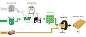
Multilayer PCB is made of copper-clad core board (Core), prepreg (PP) and copper foil, which are combined according to the lamination design and pressed together.
Before starting the PCB design, Layout engineers will determine the number of PCB layers based on the size of the circuit board, the scale of the circuit and the electromagnetic compatibility (EMC) requirements, then determine the layout of the components, and finally confirm the division of the signal layer, power layer and ground layer .
PCB stackup design principles
PCB stackup needs to be considered from many aspects such as number of layers, signal type, board thickness, material selection, copper thickness, impedance control, EMI/EMC shielding, thermal management, cost and testability.
Meets signal integrity requirements for high-speed signal cabling
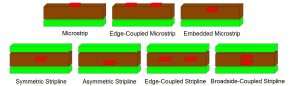
For key signal lines, it is necessary to build a stack combination of GND/Signal/GND, striplines of adjacent signal layers, and cross-vertical wiring to minimize crosstalk coupling. From the perspective of signal integrity, critical high-speed signals use stripline (Stripline) wiring, and non-critical high-speed signals can choose to use microstrip line (Microstrip) wiring.
If it is not necessary, it is not recommended to use Broadside-Coupled Stripline. Exposure and etching offsets during PCB processing will cause overlapping misalignment, making the processing process difficult and making it difficult to ensure impedance consistency.
Selection of PCB sheets, PP and copper foil
FR-4 can meet the needs of most PCBs. It is cheap and has good electrical performance. High-speed PCBs will use high-speed boards, such as Panasonic’s Megtron4/6, etc. RF PCBs will use hydrocarbon , Teflon or ceramic substrates. For example, in design scenarios with high heat dissipation requirements, such as automotive light panels, aluminum-based or copper-based plates will be used, while in display scenarios such as Mini LED, glass-based plates will be used.
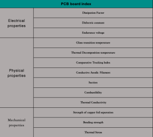
The key performance indicators of the board are as follows:
High-speed PCB board selection
High-speed PCB requires the selection of dielectric materials with the lowest loss tangent and small dielectric constant. The design of high-speed PCB requires special attention to material details, including fiberglass, dielectric matrix and copper. Signals at higher data rates have higher frequency units, shorter wavelengths, and impedance discontinuities that create more reflections. The glass fiber effect and the surface roughness of the copper foil need to be considered.
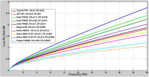
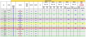
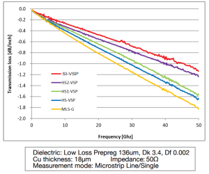
Signal attenuation of different types of boards
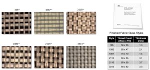
The fiberglass effect brought by fiberglass cloth
Different glass fibers have different braiding thicknesses, and the thickness of the windows and interweaving are also different. If the signals are distributed on the windows and on the glass fiber, the characteristics (impedance, delay, loss) will also be different (opening). Caused by the different Dk/Df characteristics of windows and fiberglass), this is the fiberglass effect.
Methods to alleviate the fiberglass effect:
Choose fiberglass type materials that minimize the resin window;
Use 10° routing methods such as Zig-Zag;
Let the board factory rotate a certain angle when making boards;
Use flat fiberglass cloth or plain woven cloth.
Copper foil roughness
The roughness of the copper foil (copper teeth) makes the width and line spacing of the lines uneven, resulting in uncontrollable impedance. At the same time, due to the skin effect, the current is concentrated on the surface of the conductor, and the surface roughness of the copper foil affects the length of signal transmission.
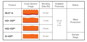
Surface roughness of different grades of copper foil
Attenuation of high-speed signals caused by copper foil roughness
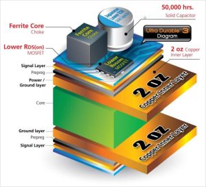
Copper thickness of each layer of PCB
The thickness of PCB copper foil is measured in ounces (oz). Common copper thicknesses come in three sizes, 0.5oz (inner layer), 1oz (surface layer) and 2oz, which are mainly used in consumer and communication products. Above 3oz is thick copper, which is often used in high-voltage, high-current power electronic products.
Stacked Impedance Control
Many interface signal lines on PCB have impedance requirements, common single-ended 50Ω, differential 100Ω, etc. Impedance control requires a reference plane, which generally requires more than four layers.
Impedance mismatch can cause signal integrity issues such as signal distortion, reflection and radiation, affecting PCB performance. The copper thickness, dielectric constant, line width, and line spacing of the traces will all affect the impedance. We can calculate the impedance according to various EDA tools, and then adjust the routing parameters according to the designed stack structure. At present, conventional board manufacturers can control the impedance at 10%.
laminated pore structure
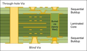
Through-holes (PTH) run throughout the PCB to connect all layers. Blind vias can connect an outer layer to one or more inner layers without passing through the PCB. Buried Via only connects the inner layer of the PCB.
High-density (HDI) PCBs often use blind vias and buried vias to optimize wiring space. Blind vias and buried vias also cause the PCB to be pressed multiple times and increase the process. PCB manufacturing becomes more difficult and therefore more expensive.
In the laminated design, the hole structure of the entire board needs to be designed according to the design needs, and the hole structure should be simplified as much as possible while satisfying the design.
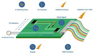
EMC design of PCB stack-up
The following principles should be followed when designing PCB stack-up EMC:
The power plane and ground plane in the board should be as close to each other as possible. Generally, the ground plane is above the power plane. This design can effectively use the interlayer capacitance as the smoothing capacitance of the power supply. At the same time, the ground plane plays a shielding role in the radiation current distributed on the power plane.
The power and ground layers are distributed in the inner layer, and the ground plane can be regarded as a shielding layer, which can well suppress the inherent common-mode RF interference on the circuit board and reduce the distributed impedance of the high-frequency power supply.
The wiring layer should be arranged as close as possible to the power or ground plane to produce flux cancellation.
Thermal Design of PCB Stackup
PCB stack design needs to consider thermal management to ensure that the heat emitted by components is effectively conducted to prevent thermal damage and improve circuit reliability. In the design process, we will first conduct thermal simulation based on the power consumption of components, optimize the component layout and design corresponding heat dissipation solutions based on the simulation results.
In the stack-up design stage, targeted heat dissipation design can also be done:
Priority is given to plates with high thermal conductivity, and metal substrates are selected as needed;
Design heat dissipation pads under high-power devices and use heat dissipation holes;
Buried copper blocks and embedded copper pillars improve heat conduction efficiency;
Increase the ground plane and pave the empty area to increase the heat dissipation area.
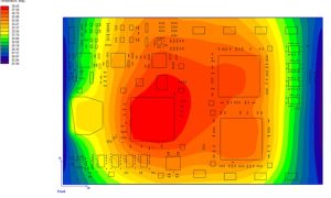
Plate thickness control
Conventional finished PCB thicknesses are 0.5mm, 0.8mm, 1.0mm, 1.2mm, 1.6mm, 2.0mm, 3.2mm, 6.4mm, etc. Generally, boards with small areas are relatively thin. Boards with frequent plugging and unplugging, large installation stress, and large areas need to be thicker from the perspective of structural reliability.
PCB stackup design steps
PCB stackup design generally follows the following steps:
1. Determine the total thickness of the stack, that is, the plate thickness;
2. Determine the number of PCB layers and assign the signal layer, ground plane layer and power layer;
3. Determine the copper thickness of the inner and outer layers;
4. Determine the distribution of impedance lines;
5. Determine the via structure;
6. Determine the residual copper rate of each layer, it is best to be symmetrical;
7. Select plate, PP and copper foil materials that meet the design requirements.
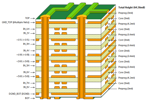
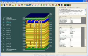
Taking a 12-layer board as an example, the designed stacked structure is as follows: