- What is Impedance Control and Signal Matching
Impedance control is matching PCB trace dimensions and locations with the
properties of the substrate material to make sure that the strength of a signal
traveling along a trace is within a required range. The continual increase in device
switching speeds is confronting engineers with signal integrity(SI) problems and
eventually, most devices are going to have to deal with SI issues. So, Printed Circuit
Board(PCB) traces can no longer be treated as a simple point-to-point connection.
Traces need to be considered as transmission lines and impedance matching
becomes necessary to lessen or eliminate the impact on SI. By following good design
practices and approaches, many potential signal integrity issues can be averted or
mitigated.
So, here we’ll talk about the importance of impedance control, the causes of signal
integrity issues, and ways to avoid them.
- WHY IS IMPEDANCE MATCHING NEEDED?
The functionof a PCB trace is to transfer the signal power from the driver device to the.
receiving device.Power needs to be propagated through out the length of the trace.
But maximum signal power can only be achieved with matching impedances on the PCB.
So, that is why there is a need for impedance matching. We want as much of the power
from the driver to end up atthe receiver. If special care is not taken in the PCB layout stage,
then high-requency signals will definitely degrade as they propagate from the driver to the
receiver. If the result of this is viewed on an eye diagram the signals will be very distorted
and power levels will be different as the signal propagates from the start to the end.
- WHAT IS A HIGH-SPEED SIGNAL OR CIRCUIT?
IPC defines a high-speed signal as one when the rise and fall time of a signal is fast
enough that the signal can change from one logic state to the other in less time than it
takes for it to travel the length of the conductor and back. So, as the signal propagates
from the source to the receiver and back – if the rise and fall time is faster than that, then
you definitely are dealing with a high-speed design and have to consider high-speed issues.
A misconception is that the clock speed of the circuit determines whether the circuit is
operating at high speed.
- WHAT ARE SOME OF THE FACTORS AFFECTINGIMPEDANCE?
Some of the variables on which the impedance of a trace is dependent on are more
or less fixed by the PCB manufacturer and some of them are defined by the PCB
designer.Power is transmitted uniformly across the length of the trace across the
PCB when there is uniform impedance.
Therefore, a trace that has a very uniform cross-sectional geometry needs to be
constructed.
In other words, the shape and size should be as uniform as possible running across a
consistent dielectric constant of the material that it’s running along the length for a
given routing layer. And the more uniform the trace the more consistent the dielectric
constant and we will achieve more consistent impedance and less power degradation.
Critical issues can arise if impedance matching is not performed.
This diagram shows a microstrip.
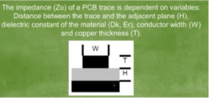
H representsthe distance between the trace and the adjacent plane. T is the trace
height orcopper thickness. Typically, this will be 35 or 70 microns depending on how
the stack-upis defined.
“W”is the width of the trace. Among these 3 variables, the trace width I the one
that is within the complete control of the designer.
A targeted impedance on a PCB trace can be attained by varying its width.
It’s important to note that the voltage may vary significantly as it is propagated along
the trace.
The presence of an impedance change or discontinuity will certainly cause a
reflection back to the source of that signal.
A major issue with boards that don’t have impedance matching is the presence of
reflections.So some of the energy of the signal will reflect toward the driver and the
remaining signal will continue onward. When you look at the waveform for this, a pure
square wave will not be seen. Rather a distorted waveform with overshoots and
undershoots and some ringing will be observed. Any unmatched impedances on the
PCB will result in some electromagnetic interference (EMI). As a result, the miss-
match of the impedance will cause some electro magnetic radiation in that localized
area where this transition occurs, and where these reflections appear.
The radiationcan couple its energy to neighboring traces or, affect some susceptible
components onthe board.
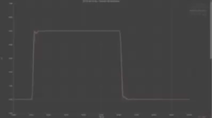
The graph on the left shows a net with potential signal integrity issues, the graph on
the right is the same net with a theoretical series termination resistor of approximately
40 ohms added.
Consider atrace, where the impedance measures 40 ohms. When this trace enters
another layer,the impedance goes up to 50 ohms, due to the geometry of the PCB. In
this case, we will have some energy reflected at the transition point. So, reflection
problems will be seen at that point and serious signal integrity issues can be
encountered in high-speed designs.
When routing the PCB, special attention needs to be paid to any mismatches in
impedance, and efforts should be made to ensure that impedances are maintained as
well as possible through out the part of a routed signal.
For products requiring CE and EMC approval special consideration to this point is
needed.
- How to achieve impedance matching?
Well-controlled impedance means that the trace impedance is constant at every point
along the pathon the PCB. This means that wherever the trace travels, even if it
changes layers, the impedance should be the same through out the part, from the
source to the destination. We don’t have much control over the impedance in the
driver or in the load but, we can control the impedance on the PCB. So, we want to
have matching circuitry on the PCB that matches the impedance of the source and
load.Therefore, we can ensure a consistent appearance throughout the entire path.
There are afew important design criteria that we need to consider. Keep in mind that
many of the problems relating to reflections relating to EMI can be prevented by good
PCB design techniques. Another crucial point is the choice of materials.
In the past,typically FR4 was specified. But with high-speed designs, the use of the
correct laminate is critical. The use of a material with a lower dielectric constant(Dk)
is advisable and preferred. This not only ensures the best signal performance, but it
will alsominimize any signal distortion or phase jitter of the signal.
From the table, you can see that material like Isola FR408 provides a consistent
dielectric constant of 3.7. So it is essential to choose the laminate material carefully.
Otherwise, you might see an inconsistency in operation between board batches: one
batch of boards might work and the next batch of boards you order might not.
Another important criterion is the loss tangent or dissipation factor. This is ameasure
of the signal loss as the signal propagates down the transmission line on the PCB. For
very high-frequency designs you would want to select the lowest loss material.
From the table, you can see that the different laminates having varying loss tangents.
So, you would need to select the material that is the most suitable for your application
and specify this in your manufacturing notes. Ensure that the bare laminate used in
the PCB fabrication process complies with IPC4101 grade. It is important to ensure
good dielectric spacing between the copper and the laminate that it is bonded to in
order to achieve a consistent electrical performance of the trace running across the
PCB.
An additional point to consider in selecting the laminate material is the fiberglass
weave pattern.A typical PCB core and prepreg substrates are constructed from
various woven fiberglass fabrics bound together with epoxy resin. The glass and
epoxy eachhave different Er/Dk values, resulting in an inhomogeneous medium for
signal propagation. A loose weave pattern produces less uniform dielectric constants
in the PCB laminate that can cause trace impedance variation and propagation skews.
The higher the frequency, the more evident this problem will be. The tighter the weave
pattern, the more uniform the dielectric constant. So, it is better to practice to choose
a tighter weave so the signal moves over more glass than anything else. The outcome
of this will be a very consistent dielectric constant throughout the PCB.
- PCB STACUP TIPS
Including power planes that can supply a signal return path below each signal path is
an essential step in controlling impedance. Preferably, these planes should be
dispersed through the board stack up and designed so a minimum of one plane
adjacent toeach signal layer is carrying controlled impedance routing.
By avoiding discontinuities (such as a split or blowout in the power plane, underneath
any criticalrouting), the return path current flowing through the plane will seek to
follow the same physical path as the route on the signal layer.
In addition to choosing the appropriate order for signal and plane layers, the material
properties of each layer need to be determined. This includes:
› Copper thickness
› Dielectric thickness
› Dielectric constant
- Other design considerations
› Trace lines should be kept as short as possible and reduce lengths wherever
possible. If the trace lengths are fairly long, terminations should be used to prevent
reflections.
› Routingstubs and discontinuities, which add to the reflections and degradation of
the signal quality, should be avoided.
› For differential pair routing, try and ensure that the signal pairs have the same length.
› Use of back drilling – for a thick back plane where the signal goes from the top
layer to one of the inner layers, the remainder of the copper barrel of the via or the
pin of the press-fit connector will be a stub, resulting in reflection. Back drilling
removes the unwanted copper. It is a technique used to remove the unused portion,
or stub, ofthe copper barrel from a thru-hole in a printed circuit board.
› Considerusing immersion silver as a surface finish rather than ENIG. Immersion
silver resultsin less insertion loss (lossy) than ENIG purely because the nickel content
in ENIG is very lossy and due to the skin effect, it is not very good for high-speed
designs. The flatness of the pad is just as good as ENIG and it is more workable than
ENIG.
› Reduce the size of anti-pads on plane layers. Anti-pads are where pads are removed,
or copper is removed on plane layers where the pad should not or does not connect
to that plane.Sometimes the anti-pad size is too large creating unnecessary voids in
the plane. By making the anti-pad a little bit smaller allows for more plane continuity
resulting in a cleaner signal and return path.
› Specify the solder mask thickness. Solder mask also has a dielectric constant. Even
thickness across the board can prevent unpleasant surprises.
› It is always a good idea to do some post design simulation or signal integrity
analysis. It’s always less expensive to fix the design before the board is
manufactured.There are some tools available to do this signal integrity analysis.
Hyperlynx is the industry standard and is very well know. Polar Instruments and Altium
Designer offer signal integrity analysis functionality.
- IMPEDANCE CONTROL VERIFICATION
Impedance control can be verified after the PCB is manufactured by using test
coupons (atest coupon is a PCB used to test the quality of a PCB fabrication
process. Test coupons are fabricated on the same panel as the PCBs, typically at the
edges. Coupons are then inspected to ensure proper layer alignment, electrical
connectivity,and cross-sectioned to inspect internal structures. Coupons can be
designed custom for a PCB or selected from a vendor library).
You can askyour PCB manufacturer to design a test coupon or ask them to place
test couponson your working panels. Typically, test coupons are placed at different
locations on the working panel, which will represent a good cross-section of the PCB.
Then, by using a Time-Domain Reflectometer (TDR) the impedance can be tested.
Subsequently,a report will be generated to indicate if the characteristic impedance
was achievedon your PCB.
The overall performance and EMC behavior of electronic equipment is not only
determined by the design of the circuitry and geometry of the layout but also by the
power distribution network.
Carefulattention needs to be paid to:
- the choice of decoupling capacitors and quantity needed and routing loops.
- the plane capacitance required by different voltages to accommodate noise limits.
- reference plane continuing and return current paths.
- inductances caused by poor component packaging.
Conclusion
With the increasing use of high-speed devices, board designers need to consider
multiple factors that could impact PCB performance. One of these considerations is
impedance control, which has serious significance on signal integrity and the
operation of the board. By understanding the causal factors for impedance mismatch
and acquiringthe knowledge of design practices that can mitigate or remove
impedance issues, the PCB designer can create a truly engineered solution. A robust
design that can be manufactured into a reliable and high performing printed circuit
board.