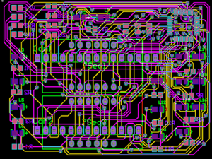
PCB boards are usually composed of multiple layers stacked together, with each layer performing a different function. The following are common PCB layers and their meanings:
Signal layer: The signal layer is one of the most important layers on the PCB board. It contains the signal transmission path between electronic components and realizes signal transmission and communication through the connection between wires and electronic components. Generally, PCB boards will have multiple signal layers for wiring and connecting complex circuits.
Stratum: The stratum is the layer designed to provide a good ground reference. It is mainly used to form a large-area ground plane to provide low noise, low impedance and electromagnetic shielding effects. The ground layer is usually located on the upper and lower sides of the signal layer to enhance signal stability and anti-interference ability.
Power Layer: The power layer is used to provide the power supply required by the circuit. It can be a positive power plane, a negative power plane, or other power planes, depending on the circuit needs. Power planes are typically used to distribute power and ground planes to reduce power supply noise and provide stable voltage and current supplies.
Planar Layer: A planar layer is a layer that has no specific electrical function and is typically used to provide mechanical support and overall structural stability. It can be an internal flat layer or an external flat layer, used to enhance the rigidity and strength of the PCB board.
Copper layer: Copper layer refers to a layer of copper material covering a specific area of the PCB board. These areas can be used to increase current capacity, provide heat dissipation, or serve as ground references. The copper layer can be an inner layer or an outer layer, depending on its location inside or outside the PCB.
Pad layer: The pad layer is located on the component mounting side of the PCB board and is used to connect and solder electronic components. The pad layer includes pads and solder pins, which are used to connect with the pins of electronic components to achieve electrical and mechanical fixation.
Silk screen layer: The silk screen layer is the layer used to print text, marks and graphics on the PCB board. It includes component location, pin identification, company logo and other information to facilitate assembly, debugging and maintenance.
Each layer has a specific function and role. In the PCB design process, reasonable layer layout and use can improve circuit performance and reliability. By properly arranging the signal layer, ground layer, power layer and plane layer, good signal integrity, power distribution and anti-interference capabilities can be achieved. The pad layer and silk screen layer facilitate the correct installation and identification of electronic components.
In summary, the meanings of each layer of the PCB board are as follows:
Signal layer: Provides signal transmission paths.
Ground layer: Provides grounding reference to enhance signal stability and anti-interference ability.
Power layer: Provides power supply.
Planar layer: Provides mechanical support and overall structural stability.
Copper layer: increases current capacity, provides heat dissipation, or serves as a ground reference.
Pad layer: connects and solders electronic components.
Silk screen layer: Print text, marks and graphics to assist assembly and maintenance.
The design and layout of these layers need to be comprehensively considered based on factors such as circuit requirements, signal integrity, and electromagnetic compatibility to ensure the performance and reliability of the PCB board.