In designing a high-speed analog signal chain, there are many options to consider for printed circuit board (PCB) layout, some more important than others and some dependent on the application. The final answer varies, but in all cases, design engineers should try to eliminate deviations from best practices without obsessing over every detail of layout and routing.
Exposed pad
Exposed pad (EPAD) is sometimes overlooked, but it is very important to get the most out of the signal chain and to adequately dissipate heat from the device.
The exposed pad, which Analog Devices calls pin 0, is the pad underneath most devices today. It is an important connection through which all the internal grounds of the chip are connected to a central point underneath the device. I wonder if you’ve noticed that many converters and amplifiers today are missing a ground pin because of the exposed pad.
The key is to properly secure (i.e. solder) this pin to the PCB to make a solid electrical and thermal connection. If this connection is not strong, confusion can occur, in other words, the design may not be effective.
Get the best connection
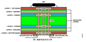
There are three steps to achieving the best electrical and thermal connection using the exposed pad. First, where possible, exposed pads should be replicated on each PCB layer. The purpose of this is to create a dense thermal connection to all ground and ground planes to quickly dissipate heat. This step is relevant for high-power devices and applications with high channel counts. Electrically, this will provide a good equipotential bonding of all ground planes.
It’s even possible to replicate the exposed pad on the bottom layer (see Figure 1), which can serve as a decoupling thermal ground point and a place to mount an underside heatsink.
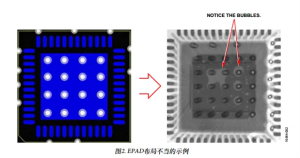
Second, divide the exposed pad into multiple identical sections, like a chessboard. Use a wire mesh cross-grid on the open exposed pad, or use solder mask. This step ensures a solid connection between the device and the PCB. During the reflow assembly process, there is no way to determine how the solder paste will flow and ultimately connect the device to the PCB.
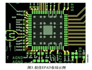
Connections may exist, but are unevenly distributed. Might only get one connection, and it’s small, or worse, located in a corner. Splitting the exposed pad into smaller sections ensures that each area has a connection point, resulting in a more secure, evenly connected exposed pad (see Figures 2 and 3).
Finally, you should make sure that each part has vias connected to ground. Each area is usually large enough to accommodate multiple vias. Before assembly, be sure to fill each via with solder paste or epoxy. This step is very important to ensure that the exposed pad solder paste does not flow back into these via voids and affect the correct connection. Finally, you should make sure that each part has vias connected to ground. Each area is usually large enough to accommodate multiple vias. Before assembly, be sure to fill each via with solder paste or epoxy. This step is very important to ensure that the exposed pad solder paste does not flow back into these via voids and affect the correct connection.
Decoupling and layer capacitance
Sometimes engineers ignore the purpose of using decoupling and simply spread many capacitors of different sizes across the board to connect the lower impedance supply to ground. But the question remains: How many capacitors are needed? Much of the literature suggests that many capacitors of varying sizes must be used to reduce the impedance of a power delivery system (PDS), but this is not entirely correct. Instead, PDS impedance can be reduced simply by selecting the correct size and type of capacitor.
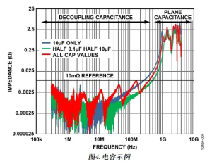
For example, consider designing a 10 mΩ reference layer as shown in Figure 4. As shown in the red curve, there are many different values of capacitors used on the system board, 0.001 μF, 0.01 μF, 0.1 μF, etc. This of course reduces the impedance in the 500 MHz frequency range, but, looking at the green curve, the same design uses only 0.1 μF and 10 μF capacitors. This proves that if the correct capacitors are used, so many capacitors are not needed. This also helps save space and bill of materials (BOM) costs.
Note that not all capacitors are “created equal”, even from the same supplier, there are differences in process, size and style. If the correct capacitors are not used, whether multiple capacitors or several different types, it will have adverse effects on the PDS.
The result may be an inductive loop. Improperly placed capacitors or using capacitors of different processes and types (and therefore respond differently to frequencies within the system) can resonate with each other (see Figure 5).
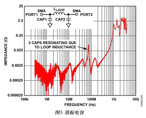
It is important to understand the frequency response of the type of capacitor used in the system. Random selection of capacitors will defeat the purpose of designing a low-impedance PDS system.
High frequency layer capacitance of PDS
To design a qualified PDS, various capacitors need to be used (see Figure 4). Typical capacitor values used on PCBs can only reduce impedance from DC or near DC frequencies to about 500 MHz. At frequencies above 500 MHz, the capacitance depends on the internal capacitance formed by the PCB. Note that it helps if the power and ground planes overlap closely.
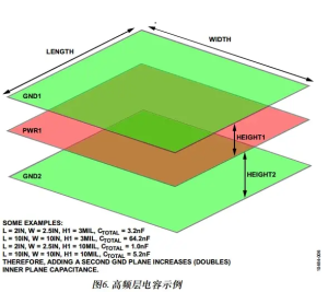
A PCB stackup should be designed that supports larger layer capacitances. For example, a six-layer stack might include a top signal layer, a first ground layer, a first power layer, a second power layer, a second ground layer, and a bottom signal layer. The first ground plane and the first power plane are specified to be close to each other in the stack-up structure, with a spacing of 2 to 4 mils between the two layers, creating an inherent high-frequency layer capacitance. The great thing about this capacitor is that it’s free, just note it in the PCB fabrication notes. If a power plane must be split, with multiple VDD rails on the same layer, the largest possible power plane should be used. Do not leave holes, and be careful with sensitive circuits. This will maximize the capacitance of this VDD layer.
If the design allows for additional layers (in the example above, going from six to eight), then two additional ground planes should be placed between the first and second power planes. With the same core spacing of 2 to 3 mils, the inherent capacitance of the stack-up structure doubles (see Figure 6 for an example).
This structure is easier to design than adding more discrete high-frequency capacitors to maintain low impedance at high frequencies.
The task of the PDS is to minimize the voltage ripple generated in response to the supply current demand, which is important but often overlooked. All circuits require current, some in larger quantities and others at a faster rate. Using well-decoupled, low-impedance power or ground planes and good PCB stackup can help minimize voltage ripple due to the circuit’s current demands. For example, depending on the decoupling strategy used, if the system is designed with a switching current of 1 A and the impedance of the PDS is 10 mΩ, the maximum voltage ripple is 10 mV. The calculation is simple: V = IR.
With a perfect PCB stack-up, the high frequency range can be covered, while the low frequency range (<500 MHz) can be covered using traditional decoupling at the power plane entry point and around high power or surge current devices. This ensures that the PDS impedance is lowest over the entire frequency range. There is no need to have capacitors everywhere; placing capacitors directly against each IC breaks many manufacturing rules. If such drastic measures are required, there is another problem with the circuit.
Layer coupling
Some layouts inevitably have overlapping circuit layers (see Figure 8). In some cases, there may be a sensitive analog layer (such as power, ground, or signal) with a noisy digital layer underneath.
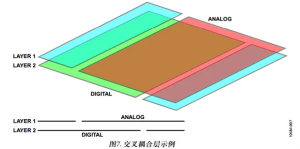
This is often overlooked because the high-noise layer is in another layer—beneath the sensitive analog layer. However, a simple experiment can prove that this is not the case. Taking a certain layer as an example, a signal is injected into any layer. Another layer is then connected, cross-coupling the adjacent layer to the spectrum analyzer. The signal quantities coupled to adjacent layers are shown in Figure 8. Even if the spacing is 40 mils, it is still capacitive in a sense and therefore will still couple signals to adjacent layers at certain frequencies.
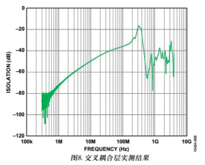
Figure 8 shows an example of this. For example, assume a high-noise digital layer on one level has a 1 V signal that switches at high speed. This means that the other layer will see 1 mV of coupling (about 60 dB isolation). For a 12-bit ADC with a 2-V p-p full-scale swing, this is 2 LSB of coupling. This may not be a problem for a particular system, but it should be noted that if the sensitivity of the system is increased by two places, from 12 to 14 bits, the sensitivity of this coupling will only increase by a factor of four, or 8 LSB.
Ignoring this type of cross-layer coupling can render the system ineffective or weaken the design. It is important to note that there may be more coupling between the two layers than imagined.
This should be noted when noise spurious coupling is found within the spectrum of interest. Sometimes the layout dictates that unintended signals or layers should be cross-coupled to different layers. Again, this should be noted when debugging sensitive systems. The problem may occur one layer below.
Separate grounding
The most common question asked by analog signal chain designers is: Should the ground plane be separated into AGND and DGND ground planes when using an ADC? The short answer is: it depends.
The detailed answer is: usually not separated. why not? Because in most cases, blindly separating the ground plane will only increase the inductance of the return path, which will cause more harm than good.
It can be seen from the formula V = L(di/dt) that as the inductance increases, the voltage noise will increase. As the inductance increases, the PDS impedance that designers have worked hard to keep down also increases. As the need to increase ADC sampling rates continues to grow, there are limited ways to reduce switching current (di/dt). Therefore, keep these ground connections unless you need to separate the ground plane.
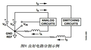
The key is that the circuit segmentation should be reasonable so that the ground layer does not have to be separated, as shown in Figure 9. Note that there is no need to separate ground planes if the layout allows you to keep the circuits within their respective areas. Such splitting provides a star ground, thereby localizing the return current to a specific portion of the circuit.
For example, when a circuit board cannot achieve good layout segmentation due to size constraints, it is necessary to separate the ground layer. This could be that dirty bus power or noisy digital circuitry must be placed in certain areas to comply with traditional design requirements or dimensions. In this case, separating the ground plane is key to achieving good performance. However, for the overall design to be effective, these ground planes must be connected together via a bridge or connection point somewhere on the board. Therefore, the connection points should be evenly distributed on separate ground planes.
Ultimately, there will often be a connection point on the PCB that becomes the best place for return current to pass through without degrading performance or forcing the return current to be coupled into sensitive circuitry. If this connection point is located at, near or beneath the converter, a separate ground is not required.
Conclusion
Layout considerations are always confusing because there are so many optimal options. Technology and principles have always been part of the company’s design culture. Engineers like to draw on experience from previous designs, while product launch pressure makes designers reluctant to make changes or try new technologies. They get wedded to risk tradeoffs until major problems arise within the system.
At the evaluation board, module, and system levels, a simple single ground is best. Good circuit segmentation is key. This also affects layer and adjacent layer layout. If the sensitive layer is above a noisy digital layer, be aware that cross-coupling may occur. Assembly is also important; the manufacturing notes provided to the PCB shop or assembly shop should be put to good use to ensure a reliable connection between the IC exposed pad and the PCB.
Poor assembly often results in poor system performance. Decoupling close to the power plane entry point and VDD pin of the converter or IC is always beneficial. However, to increase the inherent high frequency decoupling capacitance, closely stacked power and ground planes should be used (≤4 mils apart). This method comes at no additional cost and only takes a few minutes to update the PCB manufacturing notes.
When designing a high-speed, high-resolution converter layout, it is difficult to take into account all the specific features. Every application is unique. Hopefully, the few points outlined in this application note will help design engineers better understand future system designs.